Flash Adc Schematic Diagram Diy 3bit Flash Adc
Adc ic circuit diagram Diy 3bit flash adc Adc convertors integrated circuits
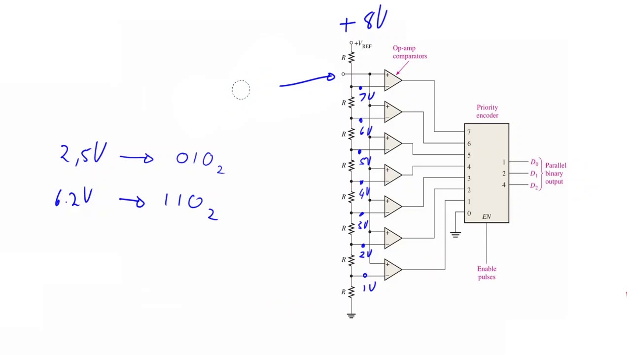
Flash ADC (3-bit) - YouTube
[diagram] 8 bit adc circuit diagram Flash adc architecture Schematic for 2-bit flash adc
Figure 1 from performance analysis of 4-bit flash adc with different
Adc flash 3bit diy circuitos electronoobsSchematic for 2-bit flash adc Analog to digital converter types4-bit flash adc circuit diagram.
Flash adc design projectVoltage divider Adc flashAdc flash parallel half.

Adc cmos adapted
Flash adcBlock diagram of flash adc (adapted from cmos circuit design, layout Flash adc (parallel adc) and half-flash adc explainedSchematic diagram of proposed flash type adc.
N-bit adc with flash architectureSolved the figure below shows a design of a 2-bit flash adc: Flash adc (3-bit)Adc resistive averaging diagram timing.

Analog to digital converters (adc) overview: working, types and
Block diagram of n-bit flash adc architectureDiy 3bit flash adc 13 block diagram of a flash adc [14]8 bit adc circuit diagram.
Adc flash bitAdc flash schematic 3bit circuit arduino voltage comparator diy circuitos electronoobs Structure diagram of flash adc. it can be seen from the working processSchematic diagram of flash adc.

Adc decoding
Flash adc speed comparators switching analogL-39 || flash type adc || 2-bit & 3-bit flash adc || explanation of Adc analog converters apogeeweb[diagram] 8 bit adc circuit diagram.
Flash type adc circuit diagram(a) schematic of 4 bit flash adc with resistive averaging. (b Flash adcThe simulated circuit design of 4-bit flash analog to digital converter.

![[DIAGRAM] 8 Bit Adc Circuit Diagram - MYDIAGRAM.ONLINE](https://i2.wp.com/d2vlcm61l7u1fs.cloudfront.net/media/5f6/5f6d8437-ba1b-4f1a-9250-f89a6701260d/phpANJPOh.png)


